
Scientists and engineers achieved the alchemist’s goal of turning low-value material, in this case sand (silicon), into gold with the invention of the MOS (metal-oxide semiconductor) transistor. According to historian David C. Brock, their creation also produced the most frequently manufactured human artifact in history.1
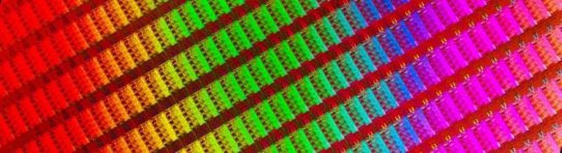
MOS transistors are microscopic electronic devices that serve as the fundamental building blocks of silicon computer chips. Millions could fit inside the period at the end of this sentence.
In 2014 industry analyst Jim Handy estimated that 2.9 sextillion transistors had been manufactured by the industry since the first one sprang to life in late 1947.2 A sextillion is one followed by 21 zeros—that’s orders of magnitude greater than the number of stars in the Milky Way. He recently updated the total to 13 sextillion. As modern graphics and artificial intelligence chips each contain billions of transistors the total continues to build at an astronomical rate.
This article acknowledges some of the pioneers who paved the initial stretches of the long and winding road that led to modern MOS technology.
The letters M-O-S describe the physical sandwich structure of the device. A Semiconducting substrate material, typically silicon, is coated with an insulating Oxide layer. Varying voltage applied to a conducting Metal electrode deposited on top of the oxide creates an electric field-effect that controls current flow through the substrate. This field-effect transistor (FET) element can perform as an amplifier, a switch, and other useful electronic functions while combining small size, low cost, and minimal energy consumption.
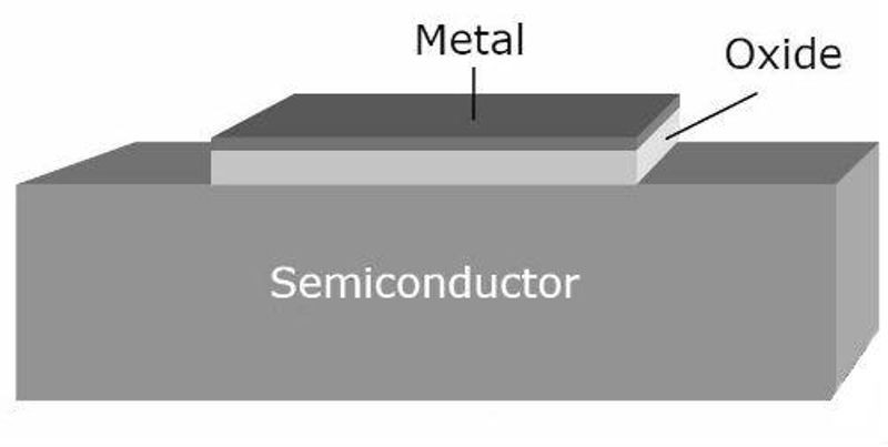
The basic metal-oxide semiconductor sandwich structure
So, who discovered MOS? Although conceptually simple, it took the contributions of numerous scientists and engineers over nearly half a century to turn the idea into a practical device. The varied acronyms used to describe the device is an indicator of the number of people and institutions across the globe that have worked on the technology. Letter salads of IGFET (insulated gate field-effect transistor), MESFET (metal semiconductor FET), MISFET (metal insulator semiconductor FET), MOSFET (metal oxide semiconductor FET), MOST (metal oxide semiconductor FET), and more littered the technical press as researchers worldwide pursued their promise. Today most settle for the simple generic name—MOS.
The technology evolved through three chronological phases; Discovery (1920s through the 1950s), Development (1960s), and Production (1970s on).
Polish-American physicist Julius Edgar Lilienfeld filed patents in Canada and the US between 1925 and 1928 describing a field-effect element that today is recognized as, an MOS transistor. Lilienfeld may not have understood the physics behind the operation of his proposed device (the first accepted “Theory of electronic semi-conductors” was not published until 1931) but co-inventor of the transistor and Nobel Prize−winner John Bardeen acknowledged in 1988 that Lilienfeld “had the basic concept of controlling the flow of current in a semiconductor.”3
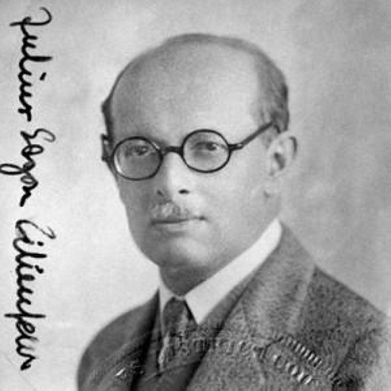
Julius E. Lilienfeld
Few know of Lilienfeld’s work. There is no evidence that he constructed functioning units and it is unlikely that he could have succeeded with the materials and equipment at his disposal.
In the late 1930s, Bell Telephone Laboratories charged William Shockley with finding a solid-state replacement for the triode vacuum tube. Unaware of Lilienfeld’s patents, he and Walter Brattain pursued field-effect experiments on copper materials employed in semiconductor rectifiers. Their research produced no successful results before being interrupted by World War II.
When Bardeen joined the project after the war, he proposed that electric charges concentrated near the surface inhibited the field-effect they were seeking. While testing his idea on germanium crystals in 1947 Bardeen and Brattain stumbled onto a different kind of transistor, called a bipolar device, that worked in the bulk of the semiconductor material far below the troublesome surface.
Shockley improved on their design with a more robust version of the bipolar transistor that appeared commercially in the early 1950s and prevailed for several decades. The trio earned the 1956 Nobel Prize in Physics for their contributions.
William Shockley, John Bardeeen & Walter Brattain
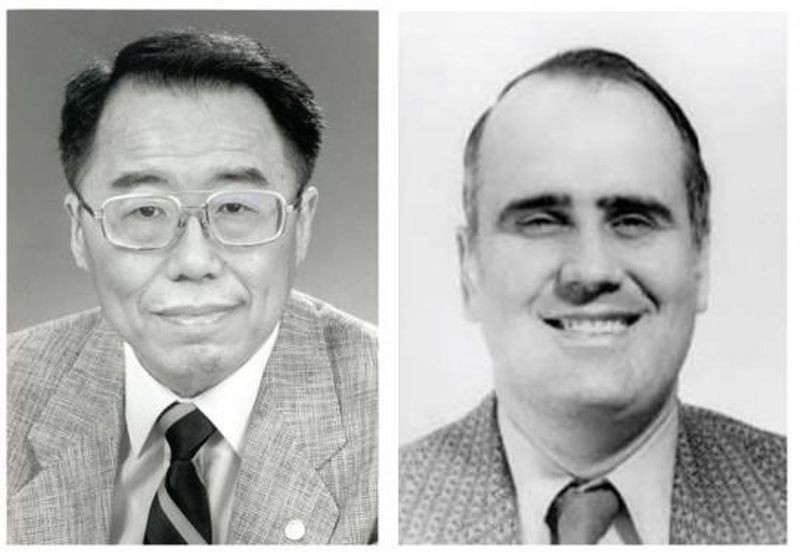
As surface conditions also contributed to problems on these early transistors, M. M. (John) Atalla headed a group at Bell that continued to research their characteristics. With improved understanding and more sophisticated equipment, 35 years after Lilienfeld documented his idea Atalla’s assistant Dawon Kahng built the first working MOS transistor. Atalla and Kahng described their work at a conference in 1960 but, as it served no immediate need in AT&T equipment, the company did not pursue development of a product.
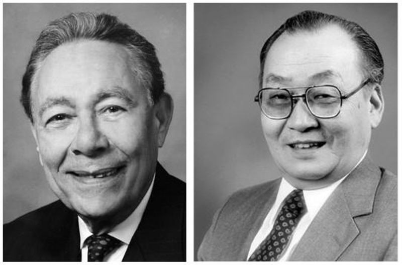
M. M. Atalla & Dawon Kahng
Learning of Bell’s success, William Webster, director of RCA’s Electronics Research Lab in Princeton, New Jersey, directed his lab personnel to duplicate the work. According to Tom Stanley, head of Integrated Electronics Research at RCA in 1960, it was seen “as an interesting niche device that might be used in some high-fidelity circuits and it would have digital application perhaps in pocket calculators and so forth. But it was slow and would never be a threat to bipolar transistors.”4
Stanley encouraged new recruit Steven Hofstein to pursue the technology because “Nobody else is working on it. A lot of people have tried to make it work... it was kind of a career killer. Nobody here will touch it with a 10-foot pole... You on the other hand have no career to kill. So why not?”5
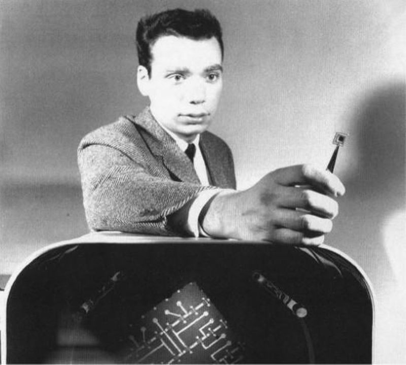
Steven Hofstein
Adopting the planar processing method recently invented by Jean Hoerni at Fairchild Semiconductor in Palo Alto, together with Fred Heiman, Hofstein built individual transistors and interconnected arrays of multiple devices—essentially the first MOS integrated circuit (IC)—in 1961.
Gordon Moore hired physicist Chih-Tang (Tom) Sah in 1959 to expand Fairchild’s silicon material and device research efforts. Sah investigated the potential of MOS and built a number of unique transistor configurations. Within three months of joining the group in 1963, newly graduated engineer Frank Wanlass conceived and patented complementary MOS that consumed zero power when not in use and identified the “floating-gate” of an MOS transistor as a memory element. These were the first of numerous variations and enhancements in the technology that were to follow. Both inventions were exploited successfully by other vendors (RCA with CMOS and Intel the EPROM, respectively) in later decades.
Andrew Grove, Bruce Deal & Edward Snow
Fairchild, RCA, and, an early Fairchild spin-out that hired Wanlass, General Microelectronics (GMe), all announced discrete MOS transistors for specialized switching and amplifier applications in 1964. GMe also introduced the first commercial MOS IC, a 20-bit shift register, and an ambitious family of custom chips for a Victor Comptometer electronic calculator.
Failure of the calculator project due to reliability and manufacturing issues with the immature process doomed GMe and delayed the advance of MOS for several years. According to Moore, “It was easy to make a device that worked, but we could not make one whose characteristics were stable. Clearly, something was happening at the silicon-oxide interface that we did not understand.”6
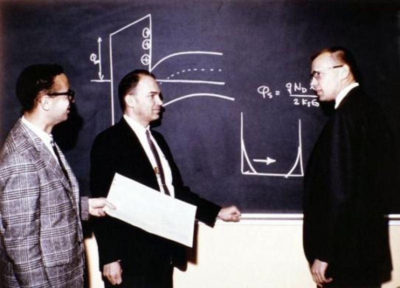
Andrew Grove, Bruce Deal & Edward Snow
Fairchild assembled teams led by Bruce Deal, Andrew Grove, and Edward Snow who conducted numerous experiments between 1963 and 1966 to address these problems. Although they were successful “Fairchild never was a major participant in the market for MOS devices . . . the main cause of this was Fairchild’s great success in bipolar circuits” as management elected to focus its efforts on maintaining that position.6
Many other US and international companies did focus on MOS as an important business opportunity. Researchers at laboratories worldwide, notably Pieter Balk at IBM Yorktown Heights and Else Kooi at Philips in Holland, contributed to improving the understanding, manufacturability, and reliability of MOS technology.
By the early 1970s the speed of operation had improved and the fundamental technical issues were resolved. MOS technology moved into the mainstream of semiconductor production and supported the creation of complex IC products, such as memories and microprocessors. It also encouraged the formation of new semiconductor companies, including Intel and Micron, to exploit the competitive advantages of small size, low cost, and low-energy consumption compared to bipolar devices.
These chips quickly enabled new classes of electronic equipment such as hand-held calculators and digital watches. Personal computers, digital communication systems, and entertainment products followed. Electronic design tools built around MOS ICs became the engines of a virtuous cycle that helped to create new semiconductor processes and devices that led to ever more sophisticated tools and successively even more powerful chips.
Five decades later the industry had shipped 13 sextillion transistors, 99.9 percent of them MOS devices. And the total increases by multiple billions every day.