
Robert N. Noyce
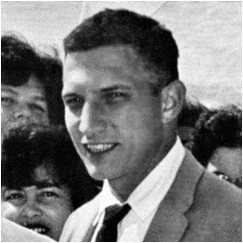
Born into a religious, mid-west farming community, a doctorate in physics from MIT, co-founder of two of the world’s most influential semiconductor companies, inventor of the modern computer chip and high-tech millionaire, in the later years of the 20th century Robert N. Noyce (1927 – 1990) was the personification of the Silicon Valley success story. Author Michael S. Malone canonized him in a 1985 profile as “St. Bob” while a Wall Street insider hailed him as a “national treasure”. Feted by presidents and honored by his peers, every janitor in town knew the legend of Bob Noyce.
While Steve Jobs and Mark Zuckerberg, the faces of contemporary Silicon Valley, are known across the world, today Noyce’s fame hardly stretches beyond Menlo Park. A new PBS documentary, to which the museum contributed material, aims to rectify that. Premiering in February 2013, American Experience: Silicon Valley spotlights the creativity of the young men who founded Fairchild Semiconductor and, in particular, Robert Noyce.
There is little I can add to the content of the PBS video, or to the excellent biography, The Man Behind the Microchip, by Leslie Berlin, or to Tom Wolfe’s classic 1983 Esquire Magazine article “The Tinkerings of Robert Noyce” to throw much new light on his life and times. However, as physical artifacts have a way of connecting us with a person or an event that goes beyond the power of words or pictures, I will describe three such items in the museum collection that help to convey a little more of the story of that brilliant, charismatic physicist.
In 1956, Noyce was recruited from his first job in solid-state research at Philco Corporation by co-inventor of the transistor William Shockley to join his start-up Shockley Semiconductor Laboratory in Mountain View, California. At Shockley Noyce earned several patents, independently discovered the tunnel diode for which Japanese scientist Leo Esaki was awarded the 1973 Nobel Prize in physics, and, most importantly, learned the arts of silicon transistor technology. Initially awed by the reputation of their brilliant but troubled leader, seven young engineers and scientists soon persuaded Noyce to jump ship with them and to found Fairchild Semiconductor Corporation just down the road in Palo Alto.
An extraordinary blend of talents in the critical skills essential for the manufacture of these new silicon devices coupled with serendipitous timing in 1957, just as the USSR launched Sputnik creating demand for sophisticated defense electronics, propelled their venture to overnight success. The ideas, people and skills that emerged from this cauldron of entrepreneurial fervor established the region as a world leader in microelectronics technology and inspired the name Silicon Valley.
The newest and most significant Noyce-related artifact in the collection is the notebook in which he kept records of patent-worthy ideas. The museum received this priceless treasure as part of the donation of over 1,000 similar volumes from Texas Instruments following the company’s acquisition of National Semiconductor in 2011. National of Santa Clara, CA had inherited the books on acquiring Fairchild Camera & Instrument Corporation in the 1980s. Key notebooks from this collection, which has been dubbed “The Dead Sea Scrolls of Silicon Valley,” will be on display to the public following processing by the museum staff.
As part of this process, I have reviewed over 200 books representing about 100 authors. No two are alike in style, content or purpose. Some were used solely for recording experimental procedures and results. Others were used as daily logs of activities or recorded detailed notes on meetings, actions item or project status. These are of course treasure troves of information for historians.
The volume issued to Noyce on February 24, 1958 is a black, cloth-bound National Figuring Book measuring 10 by 12 inches with a gold-embossed red spine and corners. It holds 152 quadrille-ruled pages on a quarter-inch grid. I am no graphologist but the bold, double-spaced cursive handwritten entries immediately conveyed the impression of a dynamic, confident author. Approximately 30 topics, ranging in length from a couple of sentences to several pages, are covered in the 93 used pages written in black ink, blue ballpoint and pencil. Most entries are titled and dated and include cross-sectional diagrams, circuit schematics, and occasional inserted Polaroid photos. Several entries deemed worthy of patent protection are signed as “Read and Understood” by his colleague Gordon Moore.
Noyce used his book for recording a stream of consciousness flow of thoughts, supporting calculations, and doodles as he worked through his ideas for new products and process improvements. To show the breadth of his curiosity, typical product ideas include a thyratron switch, a 100 MHz oscillator, a parametric amplifier resulting from a meeting with microwave entrepreneurs Watkins and Johnson, a high-efficiency photovoltaic cell and a semiconductor optical scanning device. Several of these earned patents. The crown jewel of the ideas is the concept expressed in “Methods of isolating multiple devices” dated January 23, 1959. (Figure 1 shows page 70 of the book and Figure 2, page 71) Here he took the planar process recently disclosed by his co-founder, Jean Hoerni, and extended its application to the interconnection of multiple components on a single chip. Today we know this as an integrated circuit (IC).
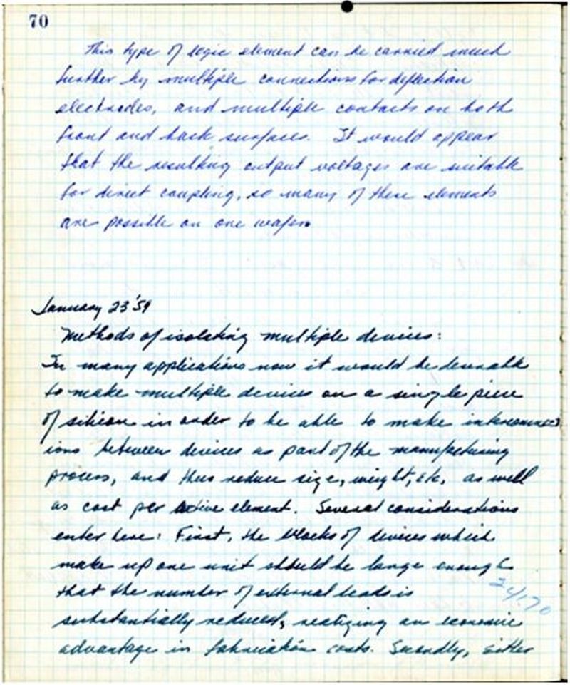
Figure 1: Robert Noyce Notebook, page 70
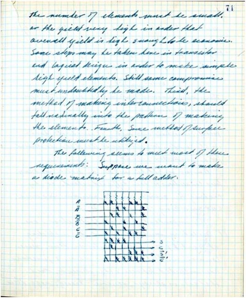
Figure 2: Robert Noyce Notebook, page 71
I was interested to discover that in an earlier idea, dated July 1, 1958, he proposed interconnecting multiple punch-through diodes on a single wafer to fabricate an integrated function table. Although this was disclosed before Jack Kilby’s solid-circuit oscillator, it suffered from the same disadvantage as approaches emanating from Bell Labs, RCA and Westinghouse in that it yielded a specialized function that could not be easily adapted for general logic purposes. However, it does illustrate that Noyce was pondering the issue of microcircuit integration before Hoerni delivered the solution. Seeing this chronological flow of ideas expressed through the hand of the inventor delivers a thrill that, given modern electronic methods of capturing and storing such ideas as they happen, will be denied to historians of our contemporary world.
The story of how this national treasure came to the Computer History Museum began in 2007. As a member of the organizing committee for the 50th anniversary celebration of the founding of Fairchild (“Fairchild@50”), I was responsible for the conference program and an exhibit of artifacts and memorabilia. I knew of the collection of notebooks owned by National and had heard that they were only accessible to the legal department and the original authors. However I thought that with appropriate security precautions we might be permitted to exhibit those of Hoerni, Moore and Noyce for a few hours to folks who knew and had worked with them. Unfortunately it did not happen. Two years later at a similar gathering to mark 50 years of the integrated circuit (“IC@50”) I decided to try again. This time we were successful and the display was one of the highlights of the event. Importantly, it helped to establish the credibility of the Museum as an appropriate repository for the books at some point in the future. Following TI’s purchase of National, led by the resourceful Rosemary Remacle and aided by the good offices of George Scalise, president emeritus of the Semiconductor Industry Association, museum personnel revived the discussions that led to the donation of all 1,334 volumes in 2012.
The concept expressed so eloquently in Noyce’s notebook in January 1959 begins on page 70:
Shortly after this disclosure, he was promoted from Director of R & D to Vice President and General Manger of the Semiconductor Division. Consequently the only effort he was able to contribute directly to the task of turning his idea into a viable product was to work with attorney John Ralls to submit a patent application in July. When issued in 1961, U. S. Patent # 2981877 “Semiconductor Device-And-Lead Structure” became one of the most frequently cited in its class and one of the most valuable in the history of the semiconductor industry.
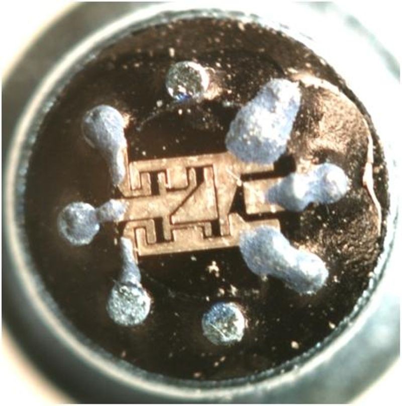
Figure 3a: Prototype version Fairchild Micrologic flip-flop, ca. June 1960
In the summer of 1959, Noyce asked fellow co-founder Jay Last to assemble a team to develop the special processes, equipment, and fabrication techniques as well as the architecture for a family of ICs they called Micrologic. Last laid out a multipronged approach that over the next 18 months led to the second group of artifacts I would like to tell you about. Figure 3a is one of the first proof-of-concept prototype IC devices delivered by Last and his team. It comprises a flip-flop built with four transistors and five resistors on single round chip of silicon mounted on a gold-plated package header. According to the notebook of team member Sam Fok, on May 12, 1960 “one unit did behave flip-flop behavior!!!” (sic) While this success did encourage their effort, it was not practical for production purposes, largely due to the use of exotic epoxy material in a critical step. The first manufacturable devices shown in Figure 3b appeared in September and were introduced to the world at an industry convention in New York in March, 1961. These photographs are of actual devices on display in the Digital Logic gallery of the Museum’s Revolution exhibit.
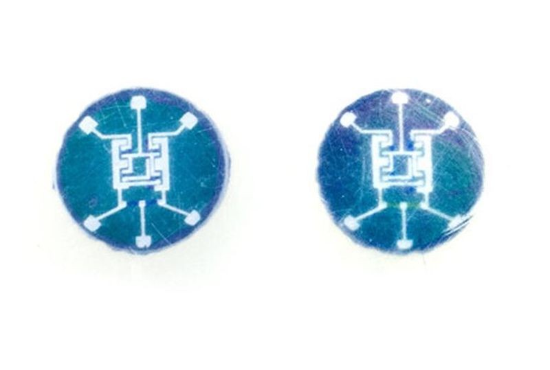
Figure 3b: Production version of Fairchild Micrologic flip-flop, ca. September 1960. CHM# 102696650
These artifacts came more easily than the notebooks. At the Fairchild@50 event I invited Jay Last and three members of his team, Isy Haas, Lionel Kattner, and Robert Norman, to participate in a group oral history of their work. Read the transcript. After the session Lionel asked if we might be interested in some of the units that he had saved from the project. Need I say more?
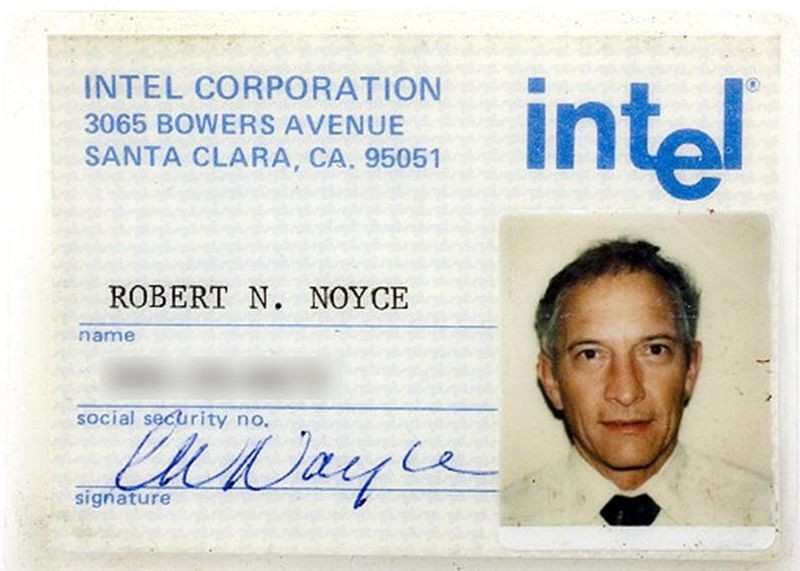
Robert N. Noyce Intel ID Card, CHM# 102716219
The last artifact I will describe is the company identification card issued to Noyce when he was CEO of Intel Corporation located on Bowers Avenue, Santa Clara, CA. It is exhibited in both the physical and online display panels on “Intel’s Microprocessor” in the Digital Logic galley of Revolution. The face of the card includes a passport style photo, his signature, and Social Security number; the number itself has been obscured by the museum staff for privacy reasons. This card was donated to the museum by Noyce’s widow Ann Bowers following a social meeting where I sat next to her at dinner. The card reminded me of the furor that arose at Fairchild in response to a memo in the museum collection written by Noyce in October 1959 that required employees to wear ID badges. In an almost apologetic tone he explained that it has “become necessary because we have grown so large so quickly that immediate face-to-face recognition is no longer possible.” No such apology would be forthcoming in our current security conscious society.