
1948: Conception of the Junction Transistor
William Shockley conceives an improved transistor structure based on a theoretical understanding of the p-n junction effect.
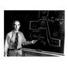
After Bardeen and Brattain's December 1947 invention of the point-contact transistor (1947 Milestone), Bell Labs physicist William Shockley began a month of intense theoretical activity. On January 23, 1948 he conceived a distinctly different transistor based on the p-n junction discovered by Russell Ohl in 1940.(1940 Milestone) Partly spurred by professional jealousy, as he resented not being involved with the point-contact discovery, Shockley also recognized that its delicate mechanical configuration would be difficult to manufacture in high volume with sufficient reliability.
Shockley also disagreed with Bardeen's explanation of how their transistor worked. He claimed that positively charged holes could also penetrate through the bulk germanium material - not only trickle along a surface layer. Called "minority carrier injection," this phenomenon was crucial to operation of his junction transistor, a three-layer sandwich of n-type and p-type semiconductors separated by p-n junctions. This is how all "bipolar" junction transistors work today.
On February 16, 1948, physicist John Shive achieved transistor action in a sliver of germanium with point contacts on opposite sides, not next to each other, demonstrating that holes were indeed flowing through the germanium. Shockley applied for a patent on the junction transistor that June and published his detailed theory of its operation in 1949. Still, it was two more years before Bell Labs scientists and engineers developed processes that allowed his junction transistor to be manufactured in production quantities (1951 Milestone).
Contemporary Documents
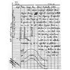
- Shockley, William. Bell Labs lab notebook No. 20455 (January 1948) pp 128-32, 23.
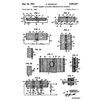
- Shockley, W. "Circuit Element Utilizing Semiconductive Material," U. S. Patent 2,569,347 (Filed June 26, 1948. Issued September 25, 1951).
- Shockley, William. "The Theory of P-N Junctions in Semiconductors and P-N Junction Transistors," Bell System Technical Journal Vol. 28 No. 3 (July 1949) pp. 435-89.
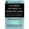
- Shockley, William. Electrons and Holes in Semiconductors with Applications to Transistor Electronics. (New York: Van Nostrand 1950).
More Information
-
Shockley, William. "Transistor Technology Evokes New Physics," Nobel lecture. Nobel Lectures, Physics 1942-1962 (Amsterdam: Elsevier Publishing Company 1964).
- Shockley, William. "The Path to the Conception of the Junction Transistor," IEEE Transactions on Electron Devices, Vol. ED-23, No. 7 (July 1976) pp. 597-620.
- Holonyak, Nick. Electrical Engineer, an oral history conducted in 1993 by Frederik Nebeker, IEEE History Center, Rutgers University, New Brunswick, NJ, USA.
- Riordan, M. & Hoddeson, L. Crystal Fire: The Birth of the Information Age. (New York: W. W. Norton 1997) pp.142-55.
Oral Histories
- Interview with William Shockley by Lillian Hoddeson on September 10, 1974, Niels Bohr Library & Archives, American Institute of Physics, College Park, MD 20740.