Title
Integrated circuit ceramic substratesCatalog Number
102688729Type
Physical objectDescription
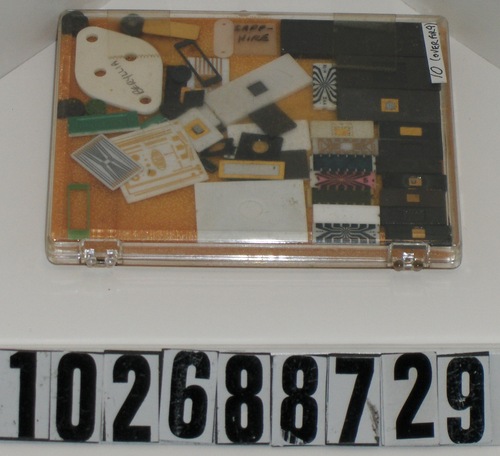
The donor describes this object as follows:"Item #I0 shows a collection of ceramic substrates that have been processed with different pattern configurations. Most of these package parts are the base, upon which the integrated circuit is mounted. In most cases, these bases require a cavity. Not shown here is the ceramic cap, which is placed over top of the base and leadframe combination, in traditional dual inline package configurations.
The black metallization pattern seen on the base of these package parts, often overplated with gold, was deposited on the ceramic by a process known as "screen printing." The metal pattern begins as a paste consisting of molybdenum and manganese powder, which is then screen printed onto the ceramic surface and fired in a hydrogen furnace at a temperature of 1500-1700°C to sinter the paste particles together, forming a continuous electrical conductor. After gold plating this pattern, the silicon chip is attached to the gold plate with a gold-silicon eutectic material, which is a conductive metallic low melting "glue." Virtually all of these ceramic piece parts were made from sintered 94% aluminum oxide, except for the beryllium oxide power flange (diamond-shaped) shown in the upper right corner. In the late 1960s, memory integrated circuits were developed that could be erased using a blast of ultraviolet (UV) light through a transparent window on the top of the package. One of these windows, made from clear sapphire, is also shown in this collection. Metal lids were often attached to these ceramic packages using a gold-tin low melting alloy stamped into the shape of a preform that looked like a metal window. This is also shown in the collection. In other cases, a low melting glass preform was used to seal certain packages, and this is shown in the green glass examples.
There are over 40 items in this accession number.
Identifying Numbers
| Other number | 10 | Key number provided by the donor is on a label on the box. |
Dimensions
in box: 1/4 in x 4 5/8 in x 3 1/2 inCategory
Component/Semiconductor/ICCredit
Gift of SEMILot Number
X4294.2008