
1974: Scaling of IC Process Design Rules Quantified
IBM researcher Robert Dennard's paper on process scaling on MOS memories accelerates a global race to shrink physical dimensions and manufacture ever more complex integrated circuits.


Linear shrinking of mask dimensions with each advance in lithographic capability provided a quick fix to enhance the speed and reduce the cost of ICs in the 1960s. Thomas Stanley of RCA Research Laboratories published an analysis in 1962 noting that this was particularly relevant to the MOS transistor because its critical speed limiting dimension, the length of the gate, lay in the horizontal rather than the vertical plane of bipolar devices.
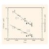
Scaling principles were described in 1972 papers by Bruce Hoeneisen and Carver Mead of Caltech and by IBM's Robert Dennard and his colleagues. But it was a 1974 paper by Dennard, et. al. that caught the attention of the industry with a resulting profound effect on microelectronics. They noted that as the horizontal dimensions of a transistor were scaled by a factor, speed improved by that same factor. At a time when IBM's MOS memories used a minimum dimension of 5 microns, they projected shrinking to fractions of a micron. (A human hair is 50-100 microns in diameter) This was the first attempt to relate a geometry shrink to the resulting power reduction and performance improvement. It gave Gordon Moore's (1965 Milestone) "Law" a scientific foundation.
In 1976 MITI organized Hitachi, NEC, Fujitsu, Mitsubishi and Toshiba into a consortium, the VLSI Technology Research Association, that embraced the concept of scaling and combined it with Japanese optical and ultra-clean manufacturing strengths in a global race to deliver 64K DRAMs (1970 Milestone) by the end of the decade. Power consumption at these high transistor counts accelerated the adoption of CMOS technology. (1963 Milestone) The ability to scale CMOS allowed dimensions to shrink below 100 nanometers (0.1 micron) by 2006 and to deliver chips such as the IBM/Sony/Toshiba 234 million transistor Cell processor for the Playstation 3.
Contemporary Documents
- Stanley, Thomas O. "The Validity of Scaling Principles for Field-Effect Transistors" David Sarnoff Research Center, Princeton Technical Report 1282 (August 13, 1962).
- Hoeneisen, B. and Mead, C. "Fundamental limitations in Microelectronics - 1. MOS Technology," Solid State Electronics, Vol. 15, No. 7 (July 1972) pp. 819-829.
- Dennard, R. H., Gaensslen, F. H., Kuhn, L., & Yu, H. N. "Design of micron MOS switching devices," IEDM Technical Digest (December 1972) pp. 168-170.
- Dennard, Robert H., Gaensslen, Fritz H., Yu, Hwa-Nien, Rideout, V. Leo, Bassous, Ernest, & LeBlanc, Andre R. "Design of ion-implanted MOSFET's with Very Small Physical Dimensions," IEEE Journal of Solid-State Circuits, Vol. 9 (October 1974) pp. 256-268.
More Information
- Sakakibara, Kiyonori. From imitation to innovation: the very large scale integrated (VLSI) semiconductor project in Japan (1983) (Massachusetts Institute of Technology, October 1983)
- Murphy, B.T., Haggan, D.E., Troutman, W.W. "From circuit miniaturization to the scalable IC," Proceedings of the IEEE, Vol. 88, Issue 5 (May 2000) pp. 691-703.
- Solomon, Paul M., Ed. "Scaling CMOS to the Limit," Special Double Issue of IBM Journal of Research and Development, Vol. 46, Number 2/3 (2002).
- Chatterjee, Pallab. "Device Scaling: The Treadmill that Fueled Semiconductor Industry Growth," IEEE SSCS Newsletter (Winter/January 2007)