
1959: Invention of the "Planar" Manufacturing Process
Jean Hoerni develops the planar process to solve reliability problems of the mesa transistor, thereby revolutionizing semiconductor manufacturing.

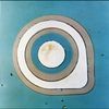
Seeking a solution to reliability issues with the mesa transistor (1958 Milestone), Fairchild physicist Jean Hoerni recalled an idea he had recorded in December 1957 - a new process in which the oxide layer is left in place on the silicon wafer to protect the sensitive p-n junctions underneath. Focused on getting its first devices into production, the company did not pursue the approach at that time. Due to concerns about possible contaminants, conventional wisdom required removing this layer after completion of oxide masking, thus exposing the junctions. Hoerni viewed the oxide instead as a possible solution - his "planar" approach, named after the flat topography of the finished device, would protect these junctions. After writing a patent disclosure in January 1959, he demonstrated a working planar transistor that March. The oxide layer was indeed found to protect the junctions, as Hoerni had predicted.
Planar devices also proved to have better electrical characteristics - particularly far lower leakage currents, which is critical in computer logic design. And they permitted fabrication of all the components of an integrated circuit from one side of a wafer (1960 Milestone). Fairchild introduced the 2N1613 planar transistor commercially in April 1960 and licensed rights to the process across the industry. The billion-transistor integrated circuits of today rely on Hoerni's breakthrough idea. One historian has called it "the most important innovation in the history of the semiconductor industry."
While planar technology enabled silicon transistors to meet the stringent demands of the aerospace industry, semiconductor vendors continued to encounter new failure mechanisms with every major technology advance. Significant issues in the 1960s included "purple plague" on gold bonding wires, electromigration of aluminum interconnect lines, and MOS transistor stability. (1964 Milestone)
Contemporary Documents
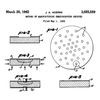
- Hoerni, J. A., "Method of Manufacturing Semiconductor Devices," U. S. Patent 3,025,589 (Filed May 1, 1959. Issued March 20, 1962). See also Hoerni's U.S. Patent No. 3,064,167.
- Hoerni, J. A., "Planar Silicon Diodes and Transistors," paper presented at the 1960 Electron Devices Meeting, Washington, D. C. - October 1960 reprinted as Fairchild Semiconductor Technical Paper TP-14. (1961).
More Information
- Lécuyer, Christophe, Making Silicon Valley: Innovation and the Growth of High Tech, 1930-1970 (Cambridge, MA: The MIT Press, 2006) pp. 150-54.
- Moore, G. M., "The Role of Fairchild in Silicon Technology," Proceedings of IEEE, Vol.86, No. 1 (January 1998) pp. 53-62.
- Selikson, B., Longo, T. A. "A Study of Purple Plague and its Role in Integrated Circuits," Proceedings of the IEEE, Vol. 52, Issue 12 (Dec. 1964) pp. 1638-1641.
- Blech A. and Sello, H. "The Failure of Thin Aluminum Current-Carrying Stripes on Oxidized Silicon." Physics of Failure in Electronics, USAF Rome Air Development Center Reliability Series Proceedings, Vol. 5, (1967) p. 496.
- Augarten, Stan. "The Most Efficient Way to Make Transistors," State Of The Art: A Photographic History of the Integrated Circuit. (New Haven & New York: Ticknor and Fields, 1983) p. 8.
- Riordan., Michael. "The Silicon Dioxide Solution: How physicist Jean Hoerni built the bridge from the transistor to the integrated circuit," IEEE Spectrum (December 2007) pp. 44-50