
1955: Development of Oxide Masking
Carl Frosch and Lincoln Derick grow a silicon dioxide film on wafers to protect their surface and allow controlled diffusion into the underlying silicon.


In early 1955 Bell Labs researchers encountered a major problem with pitting on the surface of silicon wafers during high-temperature diffusion. This problem was overcome by chemist Carl Frosch during a serendipitous accident in which the hydrogen gas carrying impurities through the diffusion furnace briefly caught fire, introducing water vapor into the chamber. The resulting "wet-ambient" diffusion method had covered the silicon surface with a layer of glassy silicon-dioxide (SiO2).
Developed further by Frosch and his technician Lincoln Derick in the ensuing months, this technique allowed semiconductor workers to seal and protect silicon wafers during the diffusion process. The two men established what impurities, such as gallium, could penetrate the oxide layer and which others (boron and phosphorus, for example) could not. They also demonstrated how to etch small openings in the layer in order to diffuse these impurities into selected portions of the silicon surface and pattern it precisely with tiny n-type and p-type regions. In 1957 they patented and published this extremely important technique.
The silicon-dioxide layer soon became essential to manufacturing transistors and later integrated circuits in high volume production via the planar processing method, (1959 Milestone) which employs this layer to protect sensitive p-n junctions in the silicon from contamination. It also doubles as an effective insulating layer atop which metal interconnections are deposited. More than any other single factor, silicon's supple, adaptable oxide layer has established it as by far the dominant material used in microchip manufacturing.
Contemporary Documents
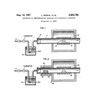
- Derick, Lincoln and Frosch, Carl J. "Oxidation of Semiconductive Surfaces for Controlled Diffusion." U. S. Patent 2,802,760 (Filed December 2 1956. Issued August 13, 1957)
- Frosch C. J. and Derick, L. "Surface Protection and Selective Masking during Diffusion in Silicon." Journal of the Electrochemical Society, Vol. 104, No. 9 (September 1957), pp. 547-552.
More Information
- Michael Riordan and Lillian Hoddeson, Crystal Fire: The Birth of the Information Age (New York: W. W. Norton, 1997) pp. 220-23.
- C. J. Frosch, "Silicon Diffusion Technology," in Biondi F. J. and Bridgers, H. E. eds. Transistor Technology, Vol. III (Princeton, NJ: D. Van Nostrand, 1958).
- Sah, C.T., Sello, H., and Tremere, D.A. "Diffusion of Phosphorus in Silicon Oxide Film." J. Phys. Chem. Solids, Vol. 11 (1959) p. 288.
- Characterization and Metrology for ULSI Technology, AIP Conference Proceedings, Vol, 683 (College Park, MD: American Institute of Physics, 2003) pp. 40-60.
- Nick Holonyak, Jr., "The Origins of Diffused-Silicon Technology at Bell Labs, 1954-55," INTERFACE (September 2007).