1960: Metal Oxide Semiconductor (MOS) Transistor Demonstrated
John Atalla and Dawon Kahng fabricate working transistors and demonstrate the first successful MOS field-effect amplifier.
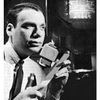
In 1959 M. M. (John) Atalla and Dawon Kahng at Bell Labs achieved the first successful insulated-gate field-effect transistor (FET), which had been long anticipated by Lilienfeld, Heil, Shockley and others (1926 Milestone) by overcoming the "surface states" that blocked electric fields from penetrating into the semiconductor material. Investigating thermally grown silicon-dioxide layers, they found these states could be markedly reduced at the interface between the silicon and its oxide in a sandwich comprising layers of metal (M - gate), oxide (O - insulation), and silicon (S - semiconductor) - thus the name MOSFET, popularly known as MOS. As their device was slow and addressed no pressing needs of the telephone system, it was not pursued further. In a 1961 memo, however, Kahng pointed out its potential "ease of fabrication and the possibility of application in integrated circuits." But researchers at Fairchild and RCA did recognize these advantages. In 1960 Karl Zaininger and Charles Meuller fabricated an MOS transistor at RCA and C.T. Sah of Fairchild built an MOS-controlled tetrode. Fred Heiman and Steven Hofstein followed in 1962 with an experimental 16-transistor integrated device at RCA.
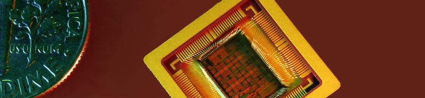
The MOS transistor conducting region is either p-type (making it a "p-channel" device) or n-type ("n-channel" device) material. The latter are faster than p-channel but are more difficult to make. MOS devices hit the commercial market in 1964. General Microelectronics (GME 1004) and Fairchild (FI 100) offered p-channel devices for logic and switching applications; RCA introduced an n-channel transistor (3N98) for amplifying signals. Because of their smaller size and lower power consumption than bipolar devices, over 99 percent of microchips produced today use MOS transistors. Achieving such ubiquity took decades of effort. (1964 Milestone)
Contemporary Documents
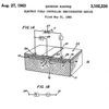
- Kahng, Dawon, "Electric Field Controlled Semiconductor Device," U. S. Patent No. 3,102,230 (Filed 31 May 31, 1960, issued August 27, 1963).
- Kahng, Dawon. "Silicon-silicon dioxide field induced surface devices," Technical memorandum issued by Bell Labs (January 16, 1961) reprinted in Sze, S.M. Semiconductor Devices: Pioneering Papers. (Singapore: World Scientific Publishing Co., 1991) pp. 583-596.
- Sah, C. T., "A new semiconductor triode, the surface-potential controlled transistor," Proceedings of the IRE, Vol. 49, No.11 (November 1961) pp. 1623-1634.
- Hofstein, S. R. and Heiman, F. P., "The Silicon Insulated Gate Field Effect Transistor," Proceedings of the IEEE, Vol. 51 (September 1963) pp. 1190 -1202.
More Information
- Atalla, M. M. et al., "Stabilization of Silicon Surfaces by Thermally Grown Oxides," Bell System Technical Journal, Vol. 38 (May 1959), pp. 749-783.
- Augarten, Stan. "A New Form of Transistor," State Of The Art: A Photographic History of the Integrated Circuit. (New Haven & New York: Ticknor and Fields, 1983) p. 12.
- Sah, C. T. "Evolution of the MOS Transistor," Proceedings of the IEEE, Vol. 76, Issue 10, (October 1988) p. 1293.
- Ross, Ian M. "The Foundation of the Silicon Age" Bell Labs Technical Journal (Autumn 1997) p. 11.
- Arns, R.G. "The other transistor: early history of the metal-oxide semiconductor field-effect transistor," IEEE Engineering Science and Education Journal. Volume 7, Issue 5 (October 1998) pp. 233-240.
- Bassett, Ross Knox. To the Digital Age. (Baltimore: The Johns Hopkins University Press, 2002) pp. 24-45.
Oral History transcripts at the Computer History Museum
- Hofstein, Steven R. (RCA, Princeton Electronics) an oral history (2011-10-28)
- Ahrons, Richard, Hofstein, Steven R., Schilling, Ron (David Sarnoff Research Center, Princeton - RCA Labs) an oral history (2011.10.28) Transcript in process
Oral Histories
- Dr. Charles W. Mueller, Electrical Engineer, an oral history conducted in 1975 by Mark Heyer and Al Pinsky, IEEE History Center, Rutgers University, New Brunswick, NJ, USA.