
In one of the most famous examples of memory recall in literature, French novelist Marcel Proust’s tasting of a “petite madeleine” cake steeped in lime-blossom tea stimulated his recollection of childhood memories. While perhaps not quite in the same league as Proust’s experience, (it resulted in his 3,000-page, seven-volume epic In Search of Lost Time, a.k.a. Remembrance of Things Past), in October 2018, Computer History Museum (CHM) Senior Curator Dag Spicer emailed me a copy of the “GEM artifact,” a new donation that triggered my own “Madeleine Moment.”
Ten years ago, while researching material on the history of Moore’s Law for the Silicon Engine online exhibit, I consulted with CHM docent Harry Sello. An alumnus of the Fairchild Semiconductor Research Laboratory in Palo Alto, California, Harry worked for Gordon Moore, then the company’s director of R&D, for several years in the 1960s. In 1965 Gordon published an article, “Cramming more components onto Integrated Circuits,” in which he noted that “The complexity for minimum component [the number transistors plus the number of resistors in the circuit] costs has increased at a rate of roughly a factor of two per year.” He then projected that “over the short term this rate can be expected to continue” and made an extrapolation over the next 10 years. Gordon continued to track and predict the annual increase in IC component count that became known as Moore’s Law.

Figure 1. Gordon Moore (1962), Director, and Harry Sello (1964), Fairchild Semiconductor Research Laboratory, Palo Alto, California.
By the mid-1970s, MOS technology largely replaced bipolar in large ICs and eliminated the need for resistive circuit components. From that point on, transistor count became the dominant factor. Due to other considerations, in 1975 he reduced the rate of increase in complexity from two per year to a doubling every two years. This rate continued for decades.
In 1967 Gordon asked Harry to prepare some 35 mm color slides illustrating this trend for an upcoming talk. Harry told me that he assembled a collection of chips that included Jean Hoerni’s 1959 single planar transistor plus the bipolar IC produced each year from 1962 to 1967 that met the minimum cost per component criterion. Looking at the image 40 years later, he identified a couple of the chips but could not recall all of the circuit types and their dates. However, as it presented a visually interesting illustration of progress over time, we decided to use the image in the exhibit under the 1965 Milestone “Moore's Law Predicts the Future of Integrated Circuits” with the caption “Several of the chips in this photo provided data points for the 1965 article.” The digital file is in the CHM collection as catalog number 102740485.

Figure 2. Photograph of chips prepared for Gordon Moore presentation in 1967.
After Harry passed away in 2017, his wife Sheila came across a piece of paper that she thought might be of interest to the Museum. In the days before email, many professionals had memo pads printed with their name that they annotated and attached to documents forwarded to coworkers. This note was from Gordon E. Moore and carried a rough sketch of seven rectangles identified with numbers and notes in his handwriting. The artifact was added to the CHM collection as catalog number 102783359.
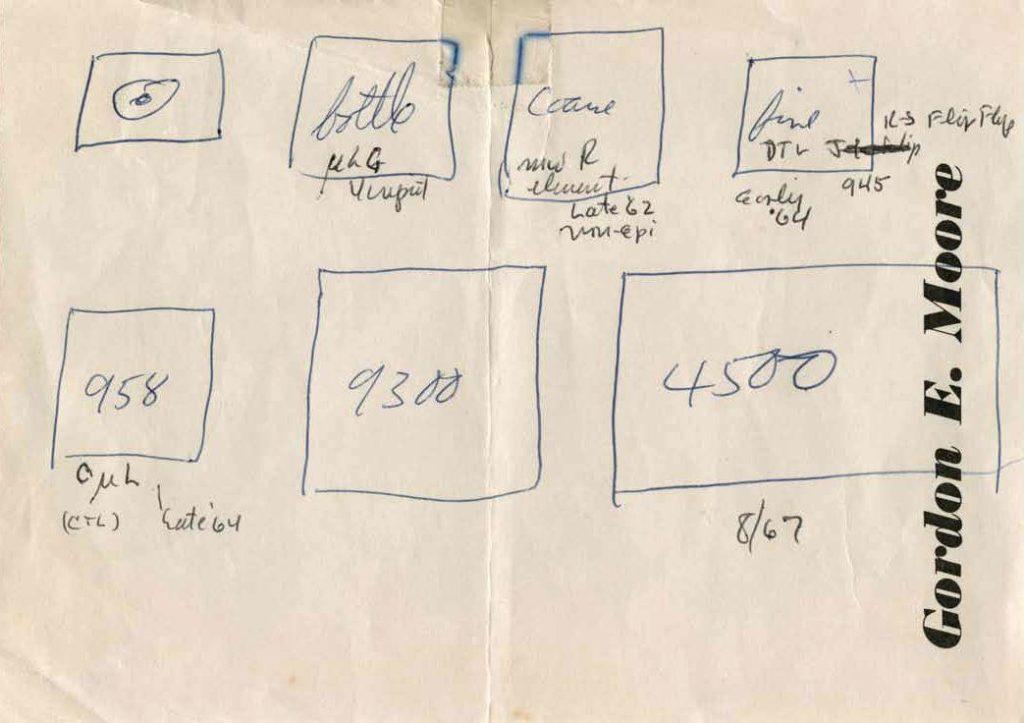
Figure 3. Gordon Moore notes on IC device types.
Under the subject “a GEM of an artifact,” Dag emailed a PDF of the sketch to curators and others at the Museum who might find it of interest. Having worked at Fairchild in the 1960s, I immediately recognized several of the part numbers from the catalog of that era. As Harry had repaired a tear in the paper and held on to it for 50 years, it must have been important to him. While trying to decipher the notes in Gordon’s (in blue ink) and Harry’s (in black ink) cryptic scrawl, something familiar about the arrangement of the rectangles triggered my Madeleine Moment. This was the Rosetta Stone to the device types in that 1967 photograph and the first five appeared to match the years of the devices on the plot of Figure 2 from the 1965 article.
From early data sheet circuit schematics and with expert help from Bob McConnell, another Fairchild alumnus, we prepared the following component count (transistors plus resistors) for each of the seven device types.
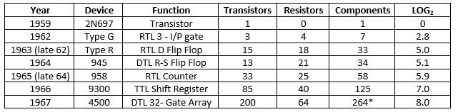
*Component count estimated from a microphotograph Figure 4. Table of component count for devices in photograph.
Figure 5a, shows Fig. 2 from the 1965 article. The vertical axis, Log to the base 2 of the number of components in each device, allowed a straight-line extrapolation of the trend into the future. Superimposing the equivalent value for each of the devices in the 1967 photograph onto the graph yields a similar plot, see Figure 5b. As four of the five points coincide with the original values it is likely that Gordon used these devices in his projection. It is also interesting to note that the additional devices for 1966 and 1967 fall right in line with his projection.
How to explain the 1963 Type R that appears as an outlier with the Log2 value of 5.0? With 33 components, it is as complex as the 1964 device. The value of 4.2 for the year 1963 on the original plot equates to 18 components on the chip. The best candidate for that is the Type S (Half Shift Register) with 10 transistors and 8 resistors. One explanation is that Harry was unable to locate a Type S for the photo and substituted a Type R that was more complex but fabricated with the same technology.

Figure 5a. Figure 2 from 1965 article.
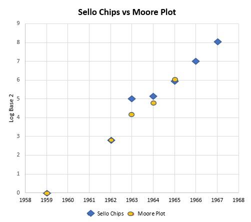
Figure 5b. Sello chips superimposed on Moore 1965 plot.
Another suggestion is that Gordon’s note “Coarse” in the third box and “fine” in the fourth may refer to the generation of lithography employed. As both devices have essentially the same component count, he may have chosen the Type R to demonstrate the benefit of finer (smaller) geometry dimensions in reducing the die size.
This new artifact answers a question asked by historians over the years, “What devices did Gordon use for his graph?” Inscribed on this modest, almost lost and forgotten, scrap of paper were device types that formed the data points behind the conception of Moore’s Law—one of the most significant and influential scientific observations in human history and a driver of technological progress for more than 50 years.
While I may not have experienced quite the same high as Proust (“a shudder ran through me and I stopped, intent upon the extraordinary thing that was happening to me. An exquisite pleasure invaded my senses”), there was a strong sense of satisfaction at connecting these two artifacts into a complete story.