Designing Integrated Circuits

Mask Rubylith Layer for 4K DRAM
This mask layer for the Mostek MK4096 4K DRAM has been prepared for photographic reduction onto a glass plate. The design was transferred to the Rubylith film and selected areas cut and stripped by hand to create the pattern.
Designing Integrated Circuits
Integrated circuits give new meaning to the cliché, “big things come in small packages.” Each holds millions of microscopic electronic components—diodes, transistors, capacitors, and resistors—configured to amplify, condition, store, and switch electronic signals.
Packing so much in so little space is challenging. It begins with a circuit diagram that is translated into a physical layout of devices and interconnections on a chip.

Electrical circuit schematic
This electrical circuit schematic shows how the 2,300 transistors of the Intel 4004 microprocessor are interconnected. (Revision G, dated 1976)
View Artifact Detail
Mask layout drawing
An electrical schematic is translated into geometric shapes that create equivalent physical circuits on the wafer. This one is for the Fairchild Micrologic “S” half shift-register.
View Artifact Detail
Mask design check plot
This composite plot combines the separate layers of photolithographic masks used for manufacturing the Am2901 bit-slice microprocessor.
View Artifact Detail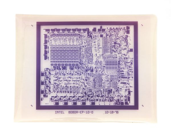

Rubylith operators
Operators hand cut IC designs onto rubylith film, which was then optically reduced to create a photographic mask.
View Artifact Detail")
Completed die photograph (QL8x12)
This photomicrograph of a Field Programmable Gate Array shows how mask layers have been successively applied to produce the finished silicon chip.
View Artifact DetailHow Many Engineers Does it Take to Design an IC?
One or two engineers armed with slide rules or calculators could design early integrated circuits. A layout person then created masks on plastic sheets, which were methodically checked and converted to glass plates used for photolithographic “printing” onto silicon wafers.
As ICs grew to millions of transistors, however, slide rules yielded to computers. Teams of engineers now design circuits, programming each step in high-level languages that automate the process.
The detailed chip layouts are now also generated automatically, having grown more complex than a street map of the entire United States.

Mainframe CAD system
A Computer Aided Design (CAD) system running on an IBM mainframe was used to design custom ICs at Fairchild in 1967.
View Artifact Detail
Engineering workstation
An IBM engineer using an integrated circuit CAD system in the 1980s.
View Artifact Detail
Introduction to VLSI systems
Lynn Conway of Xerox PARC, and Carver Mead at the California Institute of Technology, demystified the process of chip design in this classic 1979 textbook.
View Artifact Detail