From a Slice of Crystal to an IC Wafer

From Sand to Silicon: Integrated Circuit Design and Manufacturing
Our modern devices are powered by integrated circuits, tiny building blocks of the electronic world that begin, incredibly, as silicon dioxide – better known as sand. Enjoy a front row seat on the mind-blowing journey from sand to computer chip - through clean rooms, fabrication factories, and testing facilities. Hosted by industry insiders.
From a Slice of Crystal to an IC Wafer
Building an integrated circuit requires a series of manufacturing steps that introduce precise quantities of chemicals onto selected areas of the silicon wafer to form microscopic devices and interconnections. And each step must be performed in an ultra- clean environment to avoid contaminants.
Completed wafers are tested, sliced into individual chips, assembled into protective packages, and then tested again.

Silicon crystal ingot growing
Silicon ingots are grown from a single seed crystal dipped into molten (1410°C ) silicon and slowly withdrawn. The ingot is then sliced into wafers on which the IC are made.
View Artifact Detail
Metal deposition chamber
Metal is deposited onto the surface of the wafer in an evaporation chamber. It is later selectively removed by etching to form electrical interconnections between transistors.
View Artifact Detail
Wafers in a diffusion furnace
Wafers are placed in a high-temperature furnace to diffuse chemical dopants into the silicon in selective areas defined by “windows” etched through the oxide. The windows are defined by exposing light sensitive material coating the surface through the pattern printed on a photo mask.
View Artifact Detail
Weighing chemicals
Precision scales were used to measure the exact amount of chemicals needed for each step in the IC manufacturing process.
View Artifact Detail
Die assembly
The completed wafer is tested and cut into individual chips. The good devices are mounted into protective packages. Contact pads on the periphery of the IC are connected to external package leads with fine gold wires.
View Artifact DetailEvolution of the Manufacturing Process
Few industrial processes ever devised can match the complexity of manufacturing modern integrated circuits.
Early ICs were built on custom equipment costing a few thousand dollars, housed in conventional laboratories, and operated by workers in street clothes. Not any more!
As circuit dimensions shrank toward atomic levels, equipment became more sophisticated—and more expensive. Each step of the process became a specialized industry in itself.
Manufacturing now requires ultra-clean, block-long, multi- billion-dollar factories that operate with very few people present.

Wafer fabrication area
In the 1960s, operators could wear street clothes in fabrication areas because the dimensions of transistors and interconnects on an IC were much larger than typical dust particles.
View Artifact Detail
Wafer fabrication area
Modern fabrication areas require extraordinary measures to filter air and eliminate any possible contaminants. Many operations are performed in sealed modules without human operators.
View Artifact Detail
IC assembly
ICs in the 1960s typically had only 6 to 16 leads. With the aid of high quality microscopes, skilled operators were able to manipulate ultrasonic welders and attach tiny wires to contact pads and package leads.
View Artifact Detail
IC assembly
Cameras guide robots that quickly assemble ICs having hundreds of contact pads.
View Artifact DetailThe Manufacturing Process
A step-by-step process transforms a semiconductor crystal into an integrated circuit.
First, silicon wafers sawn from an ingot are polished to a mirror finish. After processing using photolithographic techniques—similar to printing processes—the completed wafer is tested, cut into individual chips, and assembled in robust packages for insertion into computer boards.
Silicon ingot (partial)
This section of a silicon ingot is what remained after the bulk of the material was sawn into 3” diameter wafers.
View Artifact Detail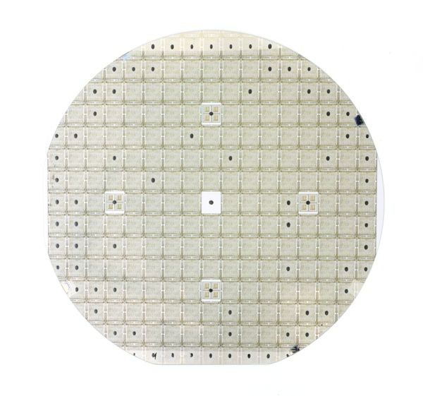
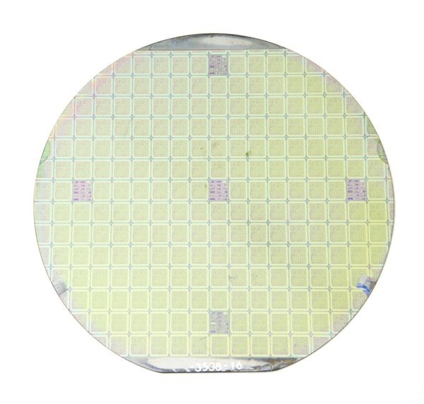
Tested wafer
After testing, the ink dots identify failed chips that will be discarded after scribing.
View Artifact Detail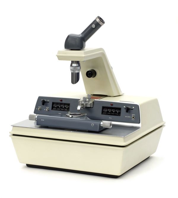
Wafer Scribing Machine
This is one of many special purpose machines needed for manufacturing ICs. It was used to scribe lines on the wafer in order to separate the chips before packaging. It won a Wescon Industrial Design award in 1965.
View Artifact Detail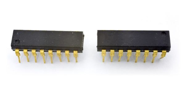
16-pin plastic dual inline packages
A completed, sealed IC package ready for insertion into a printed circuit board.
View Artifact Detail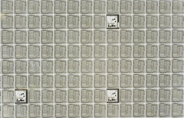
Photolithographic Masks
Masks such as these were used for the lithographic printing process for DEC Micro T11 device wafers.
View Artifact Detail