Moore's Law

Moore’s Law
The number of transistors and other components on integrated circuits will double every year for the next 10 years. So predicted Gordon Moore, Fairchild Semiconductor’s R&D Director, in 1965.
“Moore’s Law” came true. In part, this reflected Moore’s accurate insight. But Moore also set expectations— inspiring a self-fulfilling prophecy.
Doubling chip complexity doubled computing power without significantly increasing cost. The number of transistors per chip rose from a handful in the 1960s to billions by the 2010s.


Another Way To Show Moore's "Law"
The number of transistors on the largest microprocessors has doubled about every two years from 1971 to 2010.
View Artifact DetailThe Man Behind The “Law”
A Ph.D. in chemistry and physics, Gordon Moore joined Shockley Semiconductor in 1956, left with Robert Noyce and other Shockley colleagues to create Fairchild in 1957, and in 1968 co-founded Intel—serving in roles from Executive Vice President to Chairman/CEO. He became Chairman Emeritus in 1997.
Moore made his original prediction to encourage sales of ever more complex Fairchild Semiconductor chips. With new data, in 1975 he revised his prediction forecasting that IC density would double every two years. Meeting Moore’s timetable became the goal for engineers who design chips.

The birth of Moore’s Law
This is the first page of “Cramming more components onto integrated circuits,” the April 19, 1965 Electronics magazine article that introduced Moore’s Law.
View Artifact DetailBigger Wafers, Cheaper Chips
As IC chips grew larger and more densely packed with smaller transistors, the wafers they were fabricated on also grew. This combination reduced the cost per transistor from several dollars in the early 1960s to cheaper than a grain of rice today.
During the 50-year progression shown here, the smallest physical element on an IC has shrunk from 50 microns (μ) — smaller than a human hair, which is 80-100 μ in diameter — to less than 0.1 μ. (One micron is one thousandth of a millimeter, or one millionth of a meter.)
Wafer - 0.875 in, circa 1962
Wafer, smallest component dimension: 50 - 20 µ
IC Package, 6 leads, Fairchild Semiconductor, US, TO-5 metal can
View Artifact Detail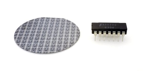
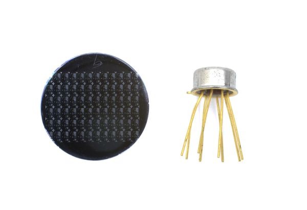
Wafer - 1.5 in, circa 1967
Wafer, smallest component dimension: about 10 µ
IC Package, 14 leads, Fairchild Semiconductor, US, Ceramic Dual-inline Package (DIP)
View Artifact Detail
Wafer - 4 in, circa 1978
Wafer, smallest component dimension: about 3 µ
IC Package, 64 leads, Amcor-Anam, Korea, Wide-body Plastic DIP
View Artifact Detail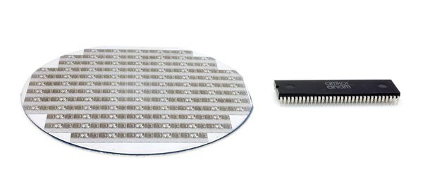
Wafer -150mm (approx 6 in), circa 1990
Wafer, smallest component dimension: about 0.8 - 00.5 µ
IC Package, 100 leads, Indy, US, Quad surface mount package
View Artifact Detail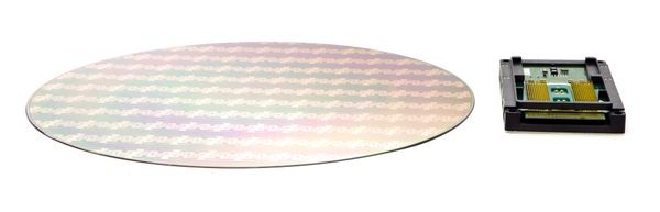
IC Package - 418 leads, Intel, 2007
Custom module for Itanium processor
Wafer, 300mm (approx 12 in), Intel Corporation, Late 2000s, Smallest component dimension: < 0.1 microns
View Artifact Detail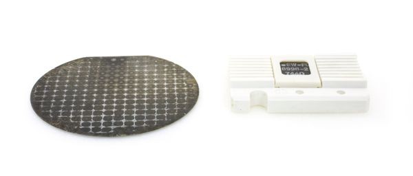
Wafer - 1.25 in, circa 1965
Wafer, smallest component dimension: about 16 µ
IC Package, 14 leads, Stewart Warner, US, Ceramic flat pack and carrier
View Artifact Detail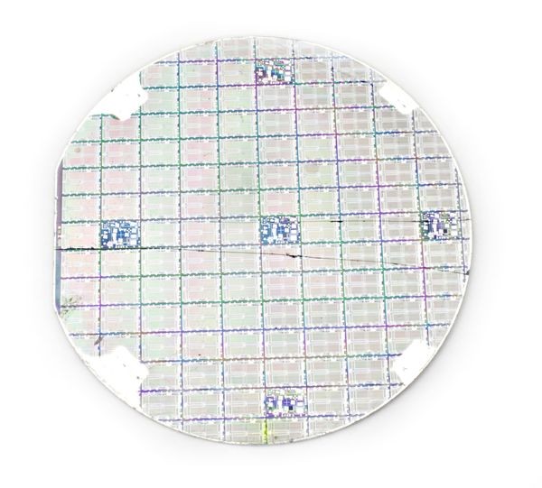
Wafer - 5 in, circa 1980
Wafer, smallest component dimension: about 1.25 - 1 µ
IC Package, 68 leads, Pin-grid array (PGA) package
View Artifact Detail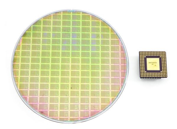
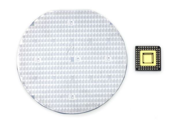
Wafer - 200mm (approx 8 in), circa 2000
Wafer, smallest component dimension: about 0.25 µ
IC Package, 162 leads, Intel Corporation, US, High-pin count PGA package with heat sink
View Artifact DetailRelated Content
Learn more about Moore’s Law
Fairchild’s Gordon Moore predicts the future of ICs
Intel information on Moore’s Law