Fairchild’s Approach: The Planar Process

First experimental planar IC
The first working experimental planar IC, built in May 1960, used an isolation technique proposed by Jay Last: deep channels were etched from the rear of the silicon wafer and filled with non-conducting epoxy.
Fairchild’s Approach: The Planar Process
The next step in IC evolution after Kilby’s “flying wire” circuits came at Fairchild Semiconductor in 1959.
Jean Hoerni’s “planar” process improved transistor reliability by creating a flat surface structure protected with an insulating silicon dioxide layer. Robert Noyce then proposed interconnecting transistors on the wafer by depositing aluminum “wires” on top. Following Noyce’s lead, Jay Last’s team built the first planar IC in 1960, spawning the modern computer chip industry.
Kilby and Noyce are considered co-inventors of the IC. Kilby alone received the 2000 Nobel Prize because Noyce had died in 1990.

Planar process patent
These figures are from Jean Hoerni’s planar process patent, “Method of manufacturing semiconductor devices” (U.S. Patent # 3.025,589) filed in May 1959.
View Artifact Detail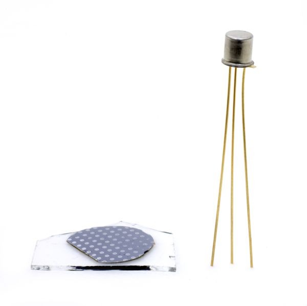
Silicon Wafer, Fairchild, 1958
This is a typical 1-inch diameter wafer from 1959, when Jean Hoerni developed the planar manufacturing process.
View Artifact Detail
CDC 6600 module with 2N709 transistor, circa 1964
This uses the first silicon transistor faster than those made from germanium. Hoerni developed the 2N709 specifically for the CDC 6600 supercomputer.
View Artifact Detail
Planar IC patent
These figures are from Robert Noyce’s planar IC patent, "Semiconductor device-and-lead structure" (U. S. Patent # 2981877) filed in July 1959.
View Artifact Detail
Micrologic Type “F” flip-flop IC, 1961
Introduced in March 1961, the early Micrologic type “F” flip-flop had a die that was etched to fit into a small, round package.
View Artifact Detail
Planar process brochure
This is the front cover of a Fairchild brochure promoting the features and benefits of the planar process to the engineering community.
View Artifact Detail, Fairchild, 1960")
Planar Transistor-Type 2N1613 (Sealed Package), Fairchild, 1960
To solve problems with Fairchild’s transistors for the Minuteman I missile computer, physicist Jean Hoerni developed the planar process. His solution saved the company and changed the industry.
View Artifact Detail
Fairchild co-founders in discussion
Robert Noyce (right) talks with his fellow co-founders in Fairchild Semiconductor’s Mountain View test area. From left: Victor Grinich Gordon Moore, Julius Blank, Eugene Kleiner, Jay Last. Jean Hoerni and Sheldon Roberts.
View Artifact Detail
The first planar IC, 1960
Jay Last’s team developed a flip-flop circuit using the new planar process. Integrating four transistors and six resistors on one chip posed many new engineering challenges. Their first prototype worked in May 1960.
View Artifact Detail
First production planar IC, 1960
This first production version of the Micrologic “F” element flip-flop planar IC was made by Isy Haas and Lionel Kattner in September 1960.
View Artifact DetailRelated Content
Learn more about Fairchild’s development of the planar integrated circuit
Jean Hoerni’s invention of the planar process
Robert Noyce’s concept of the monolithic integrated circuit
Fabrication of the first planar integrated circuit